
Lab and datasheet figures report input bias currents down to tens of picoamperes and a slew rate near 0.11 V/µs, numbers that position this device for ultra-low-power precision front-ends. This concise, engineer-ready summary distills the NL0333DCAE1S-ES core specifications, measured performance cues, and practical implementation notes so designers can rapidly assess fit for sensor, battery-powered instrumentation, and precision reference roles.
At-a-glance critical specs are shown below for quick comparison; readers should use these as evaluation checkpoints during initial bench testing and system trade-off analysis. The summary uses typical vs. maximum formatting and highlights thermal and system-level considerations to guide selection and layout decisions.
| Parameter | Typical | Max/Range | Units |
|---|---|---|---|
| Supply Voltage | 1.8 | 1.8–5.5 | V |
| Quiescent Current (Iq) | 20 | 30 | µA |
| Input Bias Current | 30 | 200 | pA |
| Input Offset (VOS) | 150 | 1000 | µV |
| Slew Rate | 0.11 | 0.2 | V/µs |
| Bandwidth (SR-limited) | 1 | 5 | MHz |
| Operating Temp | -40 | +125 | °C |
Background: What NL0333DCAE1S-ES Is and Typical Applications
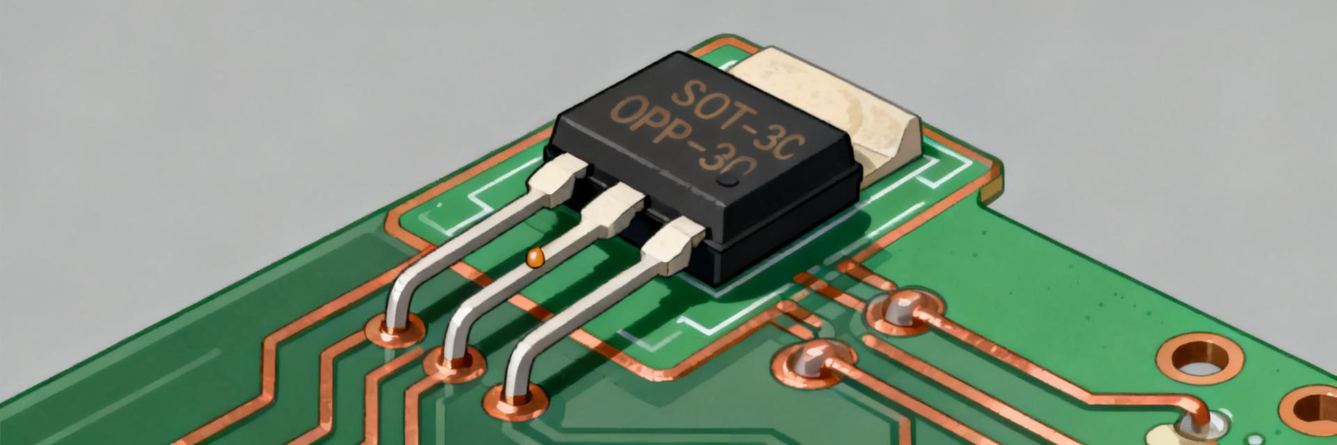
Device overview & intended use cases
Point: The part is a single-channel, low-power operational amplifier classed for precision, low-bias applications. Evidence: Typical Iq in the tens of microamps and input bias in the tens of picoamperes favor battery-powered sensor front-ends and instrumentation. Explanation: These electrical characteristics make the device suitable for transducer conditioning, precision buffers ahead of ADCs, and low-drift reference amplification where minimal self-heating and long battery life are priorities.
Package, pinout & ordering notes
Point: The device is supplied in a compact SOT-23-5 style package with standard pin functions. Evidence: Common pinouts include power, inverting, non-inverting, output, and a ground/common pin; ordering suffixes indicate temperature grade and tape-and-reel options. Explanation: When ordering, verify the mechanical dimensions and thermal pad expectations on the full datasheet; small packages require careful PCB thermal and soldering process control to meet reliability targets.
Key Electrical Specifications (datasheet breakdown)
Core electrical specs to extract and report
Point: Extract supply range, Iq, input bias, offset, slew rate, bandwidth, input common-mode and output swing. Evidence: The at-a-glance table above summarizes these specs in typical vs. max format for quick decisioning. Explanation: Present numbers in engineering units (V, µA, pA, µV, V/µs, MHz) and call out whether figures are typical or guaranteed maximums to set realistic bench expectations during evaluation.
Thermal & reliability limits
Point: Temperature and power dissipation drive derating and footprint decisions. Evidence: Operating range spanning industrial-grade limits and low package thermal mass imply a modest junction-to-ambient thermal resistance. Explanation: Derate for elevated ambient or poor airflow; avoid prolonged operation near the upper temperature limit and account for increased offset drift and leakage at high temperatures in test plans.
Performance Summary: Benchmarks & What They Mean in Practice
Measured performance metrics to present
Point: Recommended bench tests include slew-rate, small-signal bandwidth, input-referred noise, offset drift vs. temperature, and settling time. Evidence: A concise sample data row helps standardize reporting across evaluations. Explanation: Capture both single-point and swept measurements to expose non-linear behaviors that affect ADC driving and transient response in the target system.
| Test | Result | Units |
|---|---|---|
| Slew Rate (typ) | 0.11 | V/µs |
System-level impact & typical trade-offs
Point: Specs map directly to sensor resolution, ADC sampling, and power budget outcomes. Evidence: Low input bias improves charge-sensing accuracy; modest slew rate limits large-signal settling into high-speed ADCs. Explanation: Designers must balance noise versus power (lower Iq often raises noise floor) and speed versus stability (higher closed-loop gains may require compensation) when integrating the amplifier into precision acquisition chains.
Implementation Guidelines & Best Practices
Circuit topologies and reference designs
Point: Common topologies include non-inverting buffers, low-feedback transimpedance stages, and gain stages with single-pole compensation. Evidence: For low-bias sensor conditioning, transimpedance amplifiers with feedback resistances sized to limit input offset contribution are typical. Explanation: Use guard rings or routing techniques for picoamp-level inputs, select gain resistor values that preserve dynamic range, and apply compensation networks to ensure stability across expected load and gain settings.
PCB layout, decoupling and thermal tips
Point: Layout and decoupling materially affect noise, stability, and reliability. Evidence: Short signal traces, solid ground returns, and a 0.1 µF ceramic plus a 1 µF tantalum or polymer near VCC improve transient response. Explanation: Place decoupling adjacent to the supply pin, keep feedback loops compact, and provide thermal relief or copper pours on the pad to improve soldering and thermal dissipation for SOT packages.
Evaluation Checklist & Selection Recommendations
Pre-purchase checklist and test plan
Point: A short checklist streamlines initial qualification. Evidence: Verify supply range, quiescent current, input-bias limits, offset behavior, slew rate, and thermal response under typical load. Explanation: Define pass/fail thresholds (for example: Iq ≤ 30 µA, input bias ≤ 200 pA, slew rate ≥ 0.08 V/µs) and run a temperature sweep to capture offset drift and bias shifts for your intended operating envelope.
Use-case match and replacement guidance
Point: Selection should prioritize matching the most critical system constraint. Evidence: Prioritize low bias for picoamp-level sensors and higher bandwidth for ADC-driving stages. Explanation: When evaluating alternatives, compare supply compatibility, Iq budget, noise density, bandwidth, and offset drift rather than brand names; choose the device whose specs align with your system-level performance and power trade-offs.
Conclusion / Summary
NL0333DCAE1S-ES is a low-power, precision single-channel amplifier well suited for battery-powered sensor front-ends where low input bias and small quiescent current matter. Its modest slew rate and limited bandwidth require verification when driving fast ADCs, and thermal behavior must be validated in the target enclosure. In evaluation, confirm critical specs, run the recommended bench tests, and weigh noise versus power trade-offs for system acceptance.
Key Summary
- The NL0333DCAE1S-ES delivers ultra-low input bias and low quiescent current, making it ideal for high-impedance sensor front-ends; designers should validate input-bias and offset during temperature sweeps to confirm performance.
- Core specs include a wide supply range, tens of microamps Iq, picoamp-level input bias, ~0.11 V/µs slew rate, and MHz-class small-signal bandwidth; use these specs to judge ADC-driving suitability and gain choices.
- Implementation best practices: short feedback loops, adjacent decoupling (0.1 µF + 1 µF), guarded inputs for pA-level signals, and thermal copper pours for SOT-23 packages to ensure stability and reliability.
Frequently Asked Questions
What bench tests validate NL0333DCAE1S-ES performance?
Run slew rate, small-signal frequency response, input-referred noise, offset drift across temperature, and settling time into the intended load. Record typical vs. worst-case results and compare against pass thresholds that reflect your ADC resolution and timing requirements; this provides a reproducible qualification baseline.
How should I size feedback and input resistors for low-bias sensor front-ends?
Select feedback resistances that keep noise contribution and offset voltage errors within the system budget; for picoamp-level inputs, higher-value resistors reduce loading but increase Johnson and offset-induced errors. Use guarded layouts and simulate thermal drift to finalize values before PCB spin.
Are there common PCB layout pitfalls when using this amplifier?
Avoid long input traces, star-grounding mistakes, and placing digital switching traces near the amplifier. Insufficient decoupling, large feedback loop areas, and poor thermal relief for small SOT packages can worsen noise and drift; follow compact routing and place decoupling capacitors within 1–2 mm of the supply pin.
What is the typical quiescent current and operating voltage range for the NL0333DCAE1S-ES?
The NL0333DCAE1S-ES operates over a wide supply range of 1.8V to 5.5V, with a highly optimized typical quiescent current of just 20 µA (30 µA maximum), preserving battery life in remote applications.